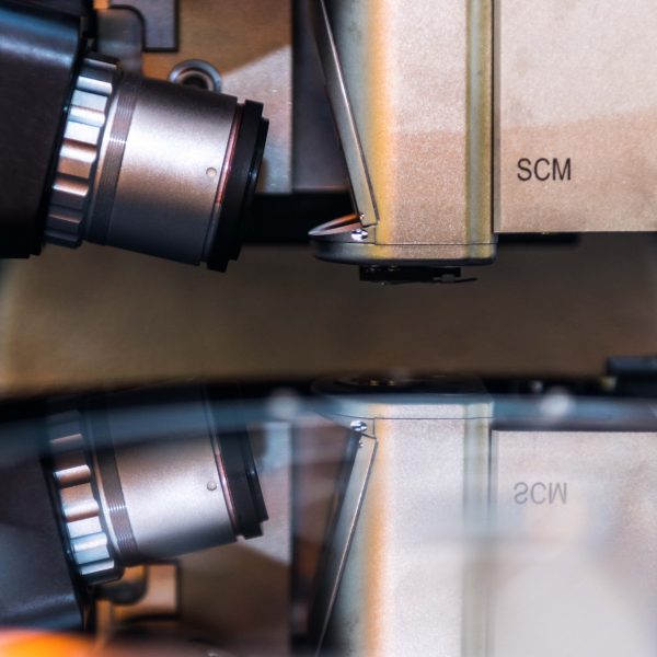
| Purpose | A metrology tool that leverages four optical modalities to image 3D topology and thin film/s properties with high automation |
| Location | Metrology Bay, RPF Cleanroom |
| Scale / volume | This microscope can accommodate samples up to 150mm diameter and 20cm in height, 3D topology mapping is limited to within a 40mm Z-range. |
| Specs / resolution | 3D topography can be mapped at a resolution down to ≈300nm in the XY plane and less than 1 nm in Z; modalities consist of confocal, three variants of interferometry, focal plane mapping, and reflectometry |
| * Not an ANFF-supported tool; access is available – refer to Access Fees schedule |
Metrology
3D Microscope Leica DCM8 *

4-point Probe

| Location | UNSW – Upper East Lab (White Area) |
| Substrates types allowed | Any |
| Substrate sizes | 30 mm x 30 mm to 2” |
| Probes | Four-point probe |
| Output | Sheet resistance for given current |
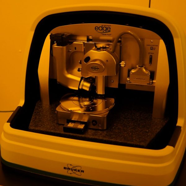
Atomic Force Microscope Bruker Icon *

| Purpose | A metrology tool that measures micron to sub-nanometre surface topology and material properties with nanometre sharp mechanical probes |
| Location | Metrology Bay, RPF Cleanroom |
| Scale / volume | This tool can accommodate 200mm wafers; maximum imaging area is 90 x 90 µm with a maximum Z-range of 10 µm |
| Specs / resolution | The resolution limit is dependent on sample and technique though generally on the order of few nm in XY and below 1nm in Z; many properties can be measured / investigated including topology, conductivity, capacitance, modulus, adhesion, etc. |
| * Not an ANFF-supported tool; access is available – refer to Access Fees schedule |
Bruker Dimension Edge AFM
| Location | UNSW – Lower East Lab (White Area) |
| X-Y Scan Range | 90μm x 90μm typical, 85μm minimum |
| Z Range | 10μm typical |
| Vertical Noise Floor | <50pm RMS |
| Sample/Size/Holder | 150mm vacuum chuck, 15mm thick |
| Scanning modes | ScanAsyst, Tapping, Contact |
| Available tips | SNL-10, RTESP-300, SCANASYST-AIR, SCANASYST-AIR-HPI, SCANASYST-FLUID, SCANASYST- FLUID+, NCHV |
Bruker Dektak Stylus profilometer
| Location | UTS |
| Description | surface height profiomter |
| Wafer size | TBC |
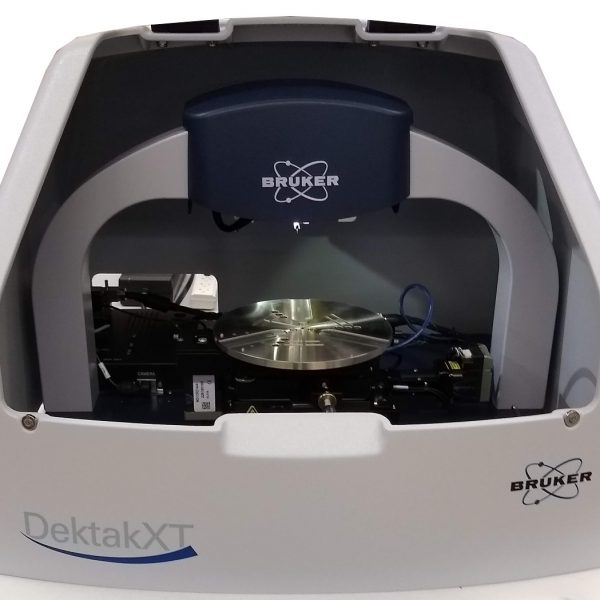
Bruker Dektak XT Stylus Profiler

| Location | UNSW – West Lab (White Area) |
| Measurement Capability | Two-dimensional surface profile measurements; Optional three-dimensional measurement/analyses |
| Sample X/Y Stage | Manual 100 mm (4 in.) X/Y, manual leveling; Motorized 150 mm (6 in.) X/Y, manual leveling |
| Data Points Per Scan | 120,000 maximum |
| Max. Sample Thickness | 50 mm |
| Step Height Repeatability | 4Å, 1 sigma on steps ≤1 μm (30 scans using a 12.5 μm stylus) |
| Vertical Range & Resolution | 1 mm, 1Å (@ 6.55 μm range) |
Cascade Probe Station

| Location | UNSW – South Lab (Test Area) |
| Model | Keithley Semiconductor Characterization system (4200SCS/C) |
| Available options | CV unit (4210-CVU),
Remote Preamp Option (4200-PA), Medium power SMU x 2 (4200-SMU), SMA to SSMC Dual with Local Ground (4200-PRB-C) |
Dektak 150

| Location | UNSW – East Lab (White Area) |
| Scan Length Range | 55 mm |
| Data Points Per Scan | 60,000 maximum |
| Max. Sample Thickness | Up to 100 mm |
| Max. Wafer Size | 150 mm |
| Height Repeatability | 6Å, 1 sigma on 1 μm step |
| Vertical Range | 524 μm |
| Vertical Resolution | 1 Å max. (at 6.55 μm range) |
| Stylus Force | 1 – 15 mg |
| Sample Viewing | 640 x 480-pixel (1/3 in.-format) camera, USB; fixed magnification, 2.6 mm FOV (166X with 17 in. monitor) |
| Sample Stage | Manual X/Y/Θ, 100 x 100 mm X-Y translation,360° rotation, manual levelling |
| Stylus radius | 6.5 µm |
Dektak 2A

| Location | UNSW – West Lab (Grey Area) |
| Sample size | From small chips up to 4” |
| Max Scan Length | 30mm |
| Max depth | 30 micron |
Ellipsometer JA Woollam M2000 *

| Purpose | A metrology tool that measures the thickness & refractive index of thin films and multi-layered films using polarised light |
| Location | Plasma Etch & Deposition Bay, RPF Cleanroom |
| Material systems | Thin films |
| Scale / volume | Small samples to 6 inch wafers |
| Specs / resolution | Measurement wavelength ranges from 200nm to 1000nm |
| * Not an ANFF-supported tool; access is available – refer to Access Fees schedule |
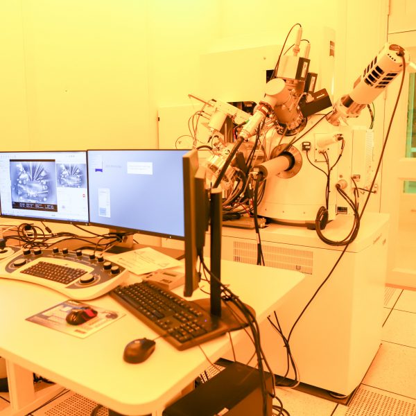
FIB-SEM Zeiss Crossbeam 550XL *
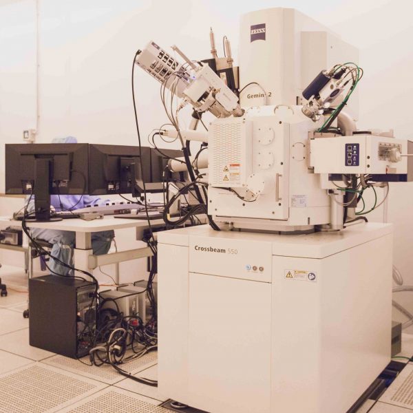
| Purpose | A multi-purpose platform that enables advanced Scanning Electron Microscopy imaging and analysis as well as Focus Ion Beam milling & deposition for cross-section profile inspection and other applications |
| Location | E-beam Bay, RPF Cleanroom |
| Material systems | It is fitted with options for elemental analysis, plasma cleaning, beam directed deposition and physical / chemical etching, diffraction based structural analysis, nano / micro manipulation, and electrical probing |
| Scale / volume | Imaging of non-conductive materials; elemental & crystallographic analysis and mapping @ ≥ 5nm; can accommodate samples as large as 150 mm wafers and 7 inch masks; 2nm image resolution; 4-10nm milling, etching, deposition |
| Specs / resolution | The FIB-SEM is a very versatile high performance tool for macro / micro / nano imaging, analysis, fabrication, manipulation, and characterisation; full analysis of any sample; in-situ milling / circuit edit / device modifications; metrology; charge compensated imaging and milling imaging; cross-sectioning; transmission imaging |
| * Not an ANFF-supported tool; access is available – refer to Access Fees schedule |
Microscope Nikon Eclipse LV100ND

| Purpose | A manual upright optical microscope with NIS Software and UV source |
| Location | Metrology Bay, RPF Cleanroom |
| Scale / volume | Can accommodate up to 150mm wafers |
| Specs / resolution | Combined reflectance / transmitted illumination with brightfield, darkfield, DIC, fluorescence, polarising, and phase-contrast; resolution limit is ≈300nm |
NanoFab Helium Ion Beam Zeiss *
| Purpose | A metrology and fabrication tool that enables imaging and fabrication at resolutions below what is possible in scanning electron microscopes |
| Location | RPF HIM Suite |
| Scale / volume | Sample sizes are limited to 50mm diameter and 30mm height |
| Specs / resolution | It is fitted with components for imaging non-conductive materials, nanoscale milling / deposition, and circuit editing; image resolution is ≈0.5nm, with ultimate limits of ≈1.5nm to 5 µm for milling / deposition |
| * Not an ANFF-supported tool; access is available – refer to Access Fees schedule |
Olympus BH2 Microscope

| Location | UNSW – Lower East Lab (White Area) |
| Sample size | From small chips up to 4” |
| Objective magnifications | 5X, 10X, 20X, 50X, 100X |
| Features | Nomarski DIC Prism available on 50X objective |
Olympus BX51 Phase Contrast & Darkfield Microscope

| Location | UNSW – West Lab (White Area) |
| Sample size | From small chips up to 4” |
| Objective magnifications | 5X, 10X, 20X, 50X, 100X |
| Features | Darkfield & Phase Contrast |
Olympus DSX1000 Digital Microscope

| Location | UNSW – West Lab (Grey Area) |
| Features | BrightField, Oblique Illumination, Darkfield, MIX Illumination, Polarization, Differential Interference Contrast Motorized XY stage, Tilting Frame including motorized Z |
| Avail. Magnifications | Zoom 140X-1400X, 30mm working distance, N,A. 0.3 Zoom 560X-5600X, 4.5 working distance, N.A. 0.8 Zoom 42-420X (long working distance) |
Optical Microscopes Olympus DSX 510 *
| Purpose | A semi-automated upright digital optical microscope with LED light source |
| Location | Metrology Bay, RPF Cleanroom |
| Scale / volume | Can accommodate up to 150mm wafers with 100mm x 100mm addressable area |
| Specs / resolution | Reflectance illumination with brightfield, darkfield, DIC, and polarising; resolution limit is ≈300nm |
| * Not an ANFF-supported tool; access is available – refer to Access Fees schedule |
Thermo G2 Phenom Bench Top SEM
| Location | UTS |
| Description | high resolution FEG benchtop SEM for ultra-fast sample loading and high quality imaging |
| Wafer size | TBC |
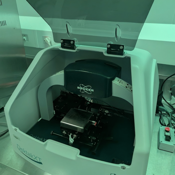
Stylus Profilometer DekTak XT *
| Purpose | The Dektak XT profilometer is a stylus profiler capable of measuring step heights, film stress, and surface roughness |
| Location | Metrology Bay, RPF Cleanroom |
| Scale / volume | Can accommodate up to 150mm wafers |
| Specs / resolution | This tool is generally used for measuring 2D profiles and has a 0.1nm vertical resolution |
| * Not an ANFF-supported tool; access is available – refer to Access Fees schedule |
J A Woollam spectroscopic ellipsometer

| Location | UNSW – West Lab (Grey Area) |
| Modes | Spectral ellipsometry, transmission measurements |
| Wavelength range | 200 – 1000nm |
| Spot size | 3x3mm |
| Stage | No scanning |
| Wafer size | Small chips up to 6” |
| Software | WASE, Complete EASE |