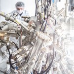
Thin Film Deposition
 Thin layers, or films, of metals, semiconductors, or dielectrics deposited on a base substrate are fundamental structural components of nano and microscale devices. ANFF-NSW has wide range of tools available for the deposition of thin films of many different materials with nanometre to micrometre thicknesses. These tools use a variety of processes to produce films with different physical and chemical properties. Physical vapour deposition (PVD) tools use thermal and electron-beam evaporation or sputtering to produce films from bulk starting materials. Chemical vapour deposition (CVD) tools such as low pressure CVD (LPCVD), plasma enhanced CVD (PECVD) and atomic layer deposition (ALD) use chemical reactions between precursor compounds or thermal decomposition of precursor chemicals to produce elemental or compound films. Depending on the deposition technique, the films can have variable density, chemical composition, internal stress, step coverage and other properties.
Dry Etching
Lithographically defined patterns with nano to microscale features sizes can be transferred into thin film layers by a number of processes. So called dry etching uses an electric discharge, or plasma, to generate ionic and radical species in a low-pressure gas or gas mixture. These species are chosen to react with particular thin film materials to create volatile compounds which are then removed, or etched, from the surface. Depending on the gas type and operating parameters, these processes are called Reactive Ion etching (RIE), Deep Trench etching (DRIE), Plasma Etching or Sputter Etching. ANFF-NSW has a range tools using all these processes which are capable of etching many materials with varying rate, selectivity to underlying or masking layers and pattern fidelity.
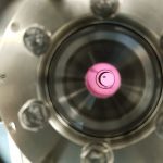
Epitaxial Growth
Epitaxial growth refers to material deposition in which crystalline layers with well-defined orientations are formed on the crystalline substrate. ANFF-NSW has both molecular beam epitaxy (MBE), as well as pulsed a laser deposition (PLD) systems. In a MBE system, a source material is heated to produce an evaporated beam of particles. These particles travel through a very high vacuum (~1e-10 mbar) and condense on the substrate. This technique is widely used for growing periodic groups III, IV, and V semiconductor crystals. Pulsed laser ablation offers another technique for epitaxial growth where high-power pulsed laser beam is used to vaporize material that deposits on a substrate.
Fibre Bragg Grating
 A Fibre Bragg Grating (FBG) is constructed with index modulation fabricated on a section of fibre by UV laser exposure. A typical application is for optical filters used in optical undersea cables which accounts for 99% of data traffic that is crossing oceans. Photonic components, modules and subsystems made by FBGs, such as fibre lasers, are also widely used. The FBG facility at the University of Sydney is based on technology developed and engineered for more than 20 years. The FBG facility can fabricate complicated FBG designs of arbitrary amplitude and phase with high fidelity and quality. FBGs are useful optical components for sensing, optical communications, and optical signal processing.
Fibre Fabrication
 Fibre fabrication is a process for making long uniform lengths of fibre, typically of dimensions between tens of microns and millimetres, and typically with complex transverse structure. This structure can provide waveguiding, or engineering mechanical, electrical, magnetic, or fluidic functionalities. It is typically a two stage process where the desired structure is assembled on macroscale, in a “preform”, and this is then drawn in a furnace down to fibre. Glasses and thermoplastics are readily drawn and can be co-drawn with some metals. The preforms may be produced by a variety of techniques including “stacking and drawing”, milling, or casting, and the fibre is drawn on a draw tower.
Lithography
The definition of etched patterns in thin films starts with the process of lithography, where the patterns are first produced in a thin overlayer of photosensitive or electron beam sensitive material. The photosensitive material, or photoresist, is exposed to UV light through a stencil mask or ‘written’ by direct exposure to a steerable, highly focussed laser beam. Electron-beam resist is written by direct exposure to a highly focussed electron beam. The exposed material has altered solubility in certain solvents called developers which can dissolve the exposed or unexposed areas of resist to leave the required pattern. ANFF-NSW has both optical and electron beam pattern generating tools capable of defining features with micro or nanoscale dimensions. Photolithographic tools are also available for exposing large area stencil or photo-masks (produced externally) or masks produced by the direct write tools. These masks can also be aligned accurately to underlying patterns to allow complex devices and structures to be fabricated
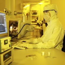
Metrology
 ANFF-NSW has a variety of tools available for monitoring and control of all stages of the fabrication of micro and nanoscale devices and structures. These include: measurement of thin film thickness; optical, mechanical and physical properties of deposited materials; dimensional measurement of patterned structures; and electrical characterisation of electronic structures. The tools available use techniques such ellipsometry, electron beam, optical and atomic force microscopy, surface profilometry, and IV and sheet resistance characterisation.
Packaging
Device packaging is the final step in the fabrication process. Packaging of a micro- or nano-electrical device allows components to be operated in applied environments by providing mechanical stability and functionality. Wire bonding allows nanoscale electrical components to communicate with the outside world, with thin electrically conductive wires allowing electricity to flow from contacts on the component to, or from, its packaging. Bonding a wafer to another wafer can help a form new functions in a device or can ensure mechanical and hermetic encapsulation of devices and electronics. Other packaging tools include dicing saws, used to separate nanofabricated devices, and probe stations, used to electrically probe nanoscale electrical components prior to mechanical and electrical packaging.
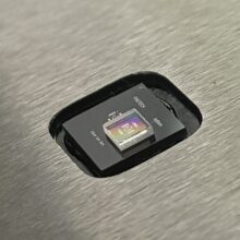
Photomask Fabrication Service
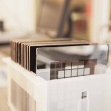
ANFF-NSW provides full service for chrome-glass photomask fabrication with client’s design and requirements. Photolithography is used to create a pattern on a substrate by shining light from a light source onto a photoresist that coats the surface of the substrate through a photomask and is followed by a development phase. Depending on the complexity of a device’s design, various deposition, etching, and lithography processes can be cycled through many times. Each mask used must be aligned perfectly to the previously processed layer if the final device is to operate as desired.
Prototyping
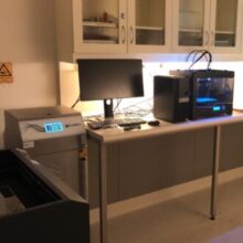
Prototyping is a quick way to produce unique parts, or for small production runs, and is useful when wanting to rapidly create prototypes with small variations in design. Prototyping capabilities include equipment which take a computer aided design model to generate components, such as laser cutters and 3D printers. 3D printing involves taking a model and slicing into layers, then printing these layers on top of one another to recreate a 3D component.
Soft Lithography
 Soft lithography is a technique used to imprint structures into mechanically soft materials from a master mould or stamp. This method of pattern transfer is used to make microfluidic devices for applications which require biocompatible materials such as Polydimethylsiloxane (PDMS). Equipment includes spin coaters (for thin layers) ovens, mixers and casting equipment.
Thermal Processing & Ion implantation
 High temperature thermal processes can be used to grow certain kinds of thin film materials, alter the stress, density or crystallinity of materials and dope materials with controlled amounts of impurities. ANFF-NSW has a range of clean furnaces and thermal reactors with temperatures capabilities up to 1200°C. These are typically used for semiconductor material processing, such as oxidation and boron and phosphorus diffusion of silicon, but some tools can be used for general annealing of thin film layers. ANFF-NSW also has an ion implantation tool that injects high-speed ions of a small range of elements into a surface to enable highly controlled doping of the surface, mostly for adjustment of the electrical resistance of semiconductor materials.
Wet Processing
The fabrication of micro and nanoscale devices requires the use of many wet chemical processes. Wet processing encompasses the processing of chemicals to clean, deposit material onto, and etch material away from substrates and components. Wet benches allow users to access solvent, caustic, and acid based processing in a safe and dedicated environment.