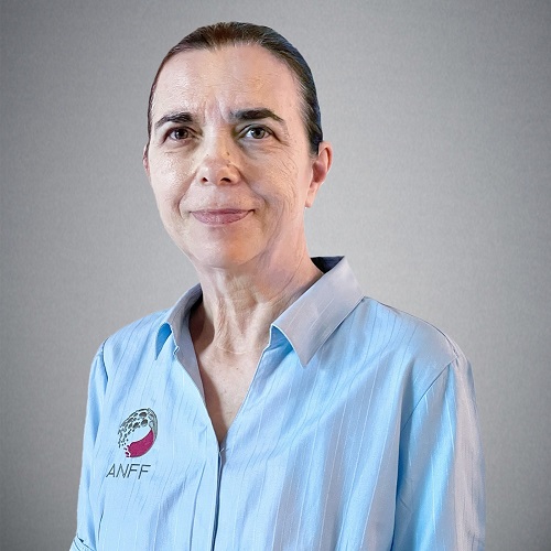
Joanna Szymanska
Process Engineerj.szymanska@unsw.edu.au
Joanna Szymanska is the process engineer responsible for technical management of semiconductor processing within ANFF Facility. Responsible for provision of training, and new microfabrication process development. As area supervisor she’s also responsible for operation and maintenance of upper east and west part of the ANFF Facility.
Her area of expertise is EBL -Raith 150TWO system, UV photolithography, RIE, ICP RIE, thin film deposition which include thermal and E-Beam evaporation, sputtering, PECVD, ALD, and thermal oxidation. She also has experience in device characterisation by profilometry, AFM, elipsometry, and probe measurements.
She gained her experience from working at CSIRO (13 years) at Marsfield cleanroom Facility mainly on fabrication and characterisation of GaAs devices, and also from the Technical University in Wroclaw in Poland (7 years) on II-V group materials.
She received her Bsc and Master degree in electronics from Technical University in Wroclaw, Poland in 1978.


