| Location | UTS |
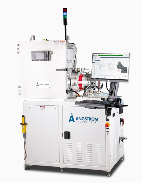
| Description | High-vacuum PVD tool with a 6-pocket electron-beam for evaporating metals and dielectrics, allowing high-purity thin-film coatings |
| Wafer size | Up to 150 mm |
Thin Film Deposition
Angstrom Electron Beam Deposition
Atomic Layer Deposition Picosun R200 *

| Purpose | A thin-film deposition tool that deposits Al2O3 and HfO2 via sequential, self-limiting process cycles with precise thickness control |
| Location | Plasma Etch & Deposition Bay, RPF Cleanroom |
| Material systems | Thermal, plasma, and ozone processes |
| Scale / volume | Small pieces up to 6 inch substrates |
| Specs / resolution | Specified to be able to deposit nitrides; techniques include thermal, plasma, and ozone processes; low temperature deposition process with uniform and conformal films |
| * Not an ANFF-supported tool; access is available – refer to Access Fees schedule |
CNT Savannah S200 atomic layer deposition system

| Location | UNSW – West Lab (White Area) |
| Materials | AlOx |
| Temperature range | 80 – 280C |
| Wafer size | Small chips up to 6” |
| Precursors | H2O, TMA |
| Restrictions | General purpose |
E-Beam Thermal Evaporator AJA ATC-1800-E *

| Purpose | A thin film deposition tool using e-beam or thermal process to deposit metal and oxides at nanometer scale thickness |
| Location | Plasma Etch & Deposition Bay, RPF Cleanroom |
| Material systems | Available materials include Ag, Al, Au, Cr, Ge, Ni, Ti, SiO2, TiO2, Ta2O, and Pt |
| Scale / volume | Small pieces to 6 inch substrates |
| Specs / resolution | Angled deposition capability; cooled rotating substrate holder; in-situ ion milling with Argon; controlled oxidation capability |
| * Not an ANFF-supported tool; access is available – refer to Access Fees schedule |
Edwards Auto 306 Thermal Evaporator (Aluminum SET)

| Location | UNSW – Lower East Lab (White Area) |
| Thin film material | Aluminium only |
| Gas | Oxygen, upper chamber for oxidation of Al only |
| Sample size | Up to 1 inch diameter (upper chamber) |
| Substrate material restriction | silicon compatible material only |
Edwards Auto 306 Thermal Evaporator (AuBe)

| Location | UNSW – Lower East Lab (White Area) |
| Thin film material | AuBe, Ti, Au |
| Base pressure | 9e-7 mbar |
| Sample size | Up to 3 inch in diameter |
| Substrate material restriction | Gallium arsenide compatible material only |
Edwards Evaporator

| Location | UNSW – South Lab (Test Area) |
| Maximum wafer size | 150 mm round |
| Throw | 400 mm |
| Boat contact size | 3/8” (~10 mm) |
| Maximum number of evaporator sources | 4 |
| Maximum power | 250 W |
| Additional process gases available | Ar, O2 |
| Other specifications | Glow discharge of process gases |
Lesker Thermal Evaporator
| Location | UNSW – South Lab (Test Area) |
| Thin film material | Ge, Ni, Ti, Au, AuGe, PdAu, Cr, Al, Co |
| Base pressure | 9e-7 mbar |
| Sample size | Up to 3 inch in diameter |
| Rotation | Angled evaporation with rotation |
Lamp Annealer ULVAC MILA 5000 *

| Purpose | A desktop annealer capable of delivering high speed heating and cooling |
| Location | Wet Etch Bay, RPF Cleanroom |
| Material systems | Gases available N2 and forming gas |
| Scale / volume | Maximum wafer size 20mm x 20mm |
| Specs / resolution | Maximum temperature of 1000°C; 50°C/s high speed heating |
| * Not an ANFF-supported tool; access is available – refer to Access Fees schedule |
Parylene Coater

| Location | UNSW – South Lab (Test Area) |
| Sample type | ALL (but contamination or hazardous ones) |
| Sample size | Up to 6” wafer (4 tiers substrates holder) |
| Adhesion promoter | Silane A-174 |
| Thickness range | 100 nm to 10um
(Thicker layer on request) |
| Dimer type | Parylene C |
Picosun R-200 ALD system

| Location | UNSW – West Lab (White Area) |
| Materials | HfO2 and Al2O3 |
| Substrate | Small chips to 200mm |
| Temperature Range | 100C – 500C |
| Precursors | H2O, TMA and TEMAH |
Seki/Astex MW-CVD diamond growth
| Location | UTS |
| Description | 1000W microwave plasma CVD system for diamond growth, primarily used for poly diamond films containing NV centres. |
| Wafer size | TBC |
| Gas available | TBC |
Sputter Coater DC Emitech K550
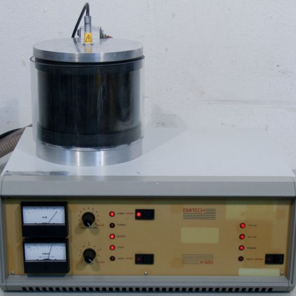
| Purpose | A small DC sputtering tool that can coat metal onto substrate |
| Location | Plasma Etch & Deposition Bay, RPF Cleanroom |
| Material systems | Available metal targets include Au, Ti, and Ni |
| Scale / volume | Small pieces to 6 inch substrates |
| Specs / resolution | Multiple small substrates for coating; coating uniformity up to 3.5 inch diameter |
Sputterer AJA ATC-2000-UHV *

| Purpose | A 5-gun DC/RF sputtering system that deposits metal and oxides at a controlled angstrom per second rate |
| Location | Plasma Etch & Deposition Bay, RPF Cleanroom |
| Material systems | Available materials include NbTi(N), SiO2, TiO2, ITO, Al, and Ti |
| Scale / volume | Small pieces to 6 inch substrates |
| Specs / resolution | Base pressure lower than 5 x10⁻⁸ torr; in-situ ion milling available; RF biased sample pre-clean available; substrate rotation with heating up to 800oC; ion milling / assisted deposition with Argon; controlled oxidation or nitration capability |
| * Not an ANFF-supported tool; access is available – refer to Access Fees schedule |
Tystar Mini-Tytan Horizontal 3 Stack LPCVD Furnace System

| Location | UNSW – East Lab (Grey Area) |
| Max capacity | 50 x 8” wafers per run, though typically 25 x 6” or 4” |
| Tube #1 | Stoichiometric and Low-Stress nitride |
| Tube #1 gases | Dichlorosilane (DCS), Ammonia (NH3), Nitrous Oxide (N2O) |
| Tube #2 | P-doped or intrinsic polysilicon, amorphous silicon, dry oxide, low temp oxide P-doped or undoped. (Dopant gas currently unavailable) |
| Tube #2 gases | Silane (SiH4), Boron Trichloride (BCl3), Oxygen (O2) |
| Tube #3 | N-doped or intrinsic polysilicon, amorphous silicon, dry oxide, low temp oxide P-doped or undoped. (Dopant gas currently unavailable) |
| Tube #3 gases | Silane (SiH4), Phosphene (PH3), Oxygen (O2) |
| Temperature range | 400C – 950C (recipe dependent) |
| Pressure range | 100 mTorr – 500 mTorr |
Lesker PVD75 e-beam evaporator - Si-MOS compatible

| Location | UNSW – West Lab (Grey Area) |
| Sample type | Silicon Only – Si-MOS Compatible |
| Sample size | Up to 4” wafer |
| Material available | Ti, Al, Pt and Pd |
| Thickness range | 1nm to 500nm |
| Option | Plasma clean capability by Ar sputtering |
Lesker PVD75 e-beam evaporator - general purpose

| Location | UNSW – West Lab (Grey Area) |
| Sample type | ALL (but contamination or hazardous ones) |
| Sample size | Up to 6” wafer |
| Material available | Metals: Ag, Al, Au, Co, Cr, Cu, Fe, Ge, Ir, Nb, Ni, NiFe, Pd, Pt, Si, Sn, Ti
Oxides: Al2O3, CeO2, Fe2O3, In2O3, SiO2, TiO2, WO3 Other materials by prior approval |
| Thickness range | 1nm to 500nm (Thicker layer on request) |
HHV sputtering system

| Location | UNSW – West Lab (Grey Area) |
| Sputter gases | Ar, N2, O2 |
| Target materials (3” targets) | Ti, Al, Cr, Au, Cu, W, Nb, Ag, Si, ITO, Si3N4, SiO2, TiO2, ZnO |
| RF power | 600W max |
| 2000W max | |
| Chamber heating | Room Temp to 400 |
| Max sample size | 6” |
| Base pressure | Mid 10-8 mtorr |
Oxford Instruments Plasmalab 100 plasma-enhanced chemical vapour deposition system

| Location | UNSW – Upper East Lab (Grey Area) |
| Materials | SiO2, SiN, a-Si:H |
| Temperature range | 100 – 300C |
| Wafer size | Small chips up to 6” |
| Gasses | SiH4, NH3, N2O, N2, Ar, CF4 |
| Restrictions | no metals |